In the microscopic world of chip manufacturing, a mask smaller than a palm determines the fate of billions of transistors. As process nodes shrink to 7nm and beyond, nanometer-scale defects—imperceptible even with advanced inspection tools—can result in significant wafer loss. This hidden risk is a daily challenge for many domestic semiconductor manufacturers.
Facing the challenge of detecting phase defects on advanced masks, coupled with the high costs and extended delivery cycles of imported equipment, the industry urgently requires a domestically produced solution that delivers nanometer-scale precision with superior cost-effectiveness.
$1.36 Billion
Projected advanced mask market for 2031①
12.2%
Compound Annual Growth Rate (CAGR)①
Class 10
requirement for high-end version
Data shows that the global advanced process mask market is growing at an astonishing rate, yet domestic manufacturers remain heavily reliant on imports for upstream materials and inspection equipment. This dependence not only drives up costs but also creates hidden risks for supply chain security. How can we achieve a breakthrough in this high-barrier technical field?
New Product Launch
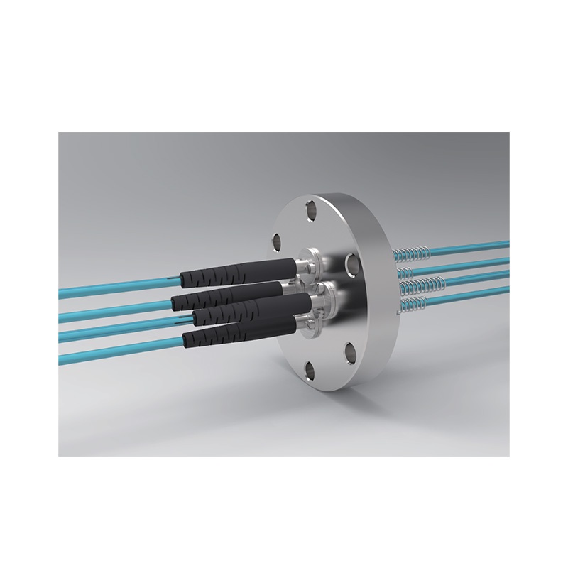
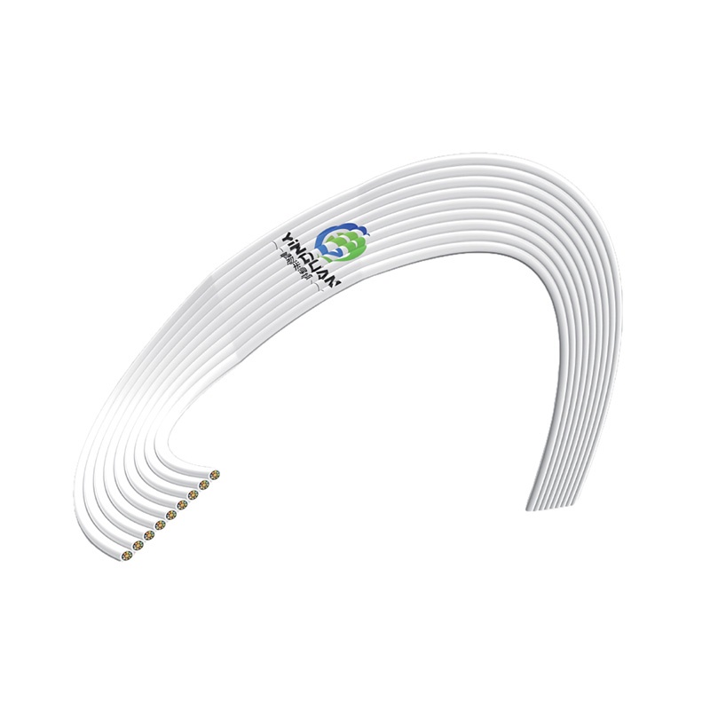
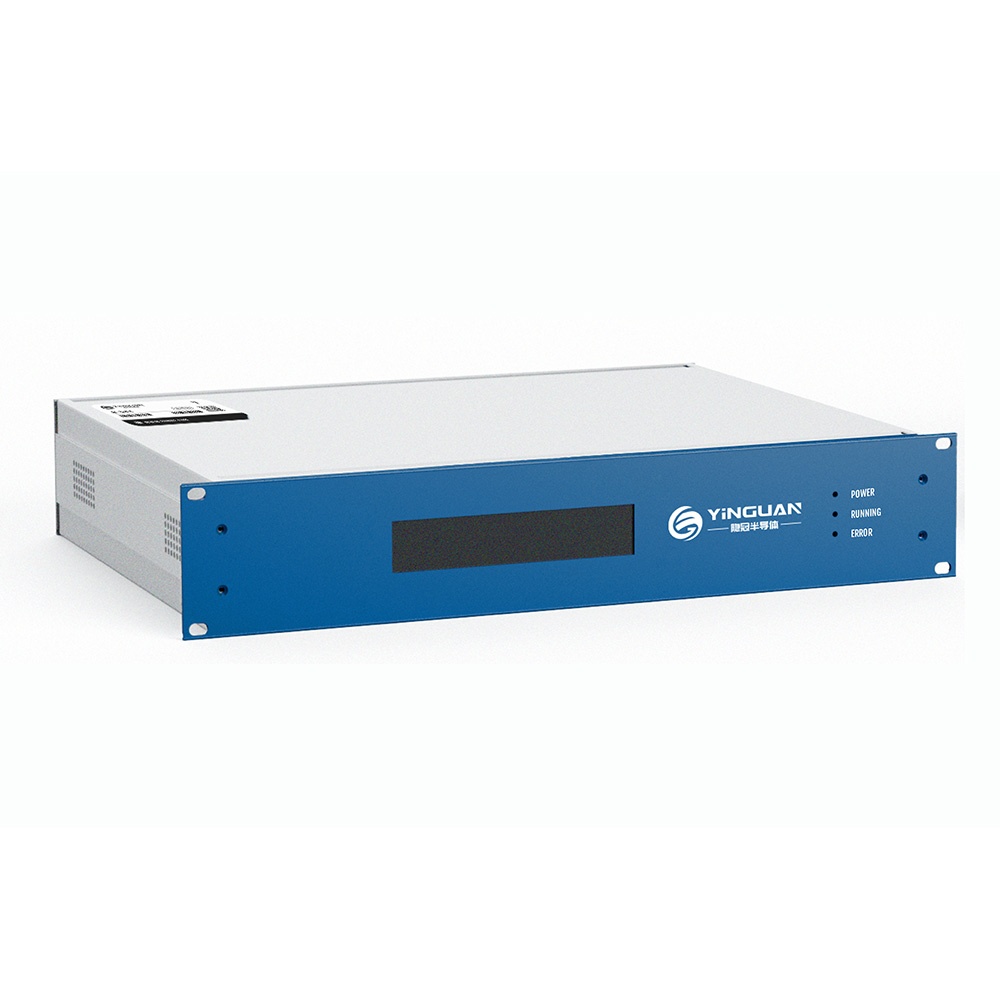
YiNGUAN Semiconductor launches a new series of precision motion stages for lithography mask inspection equipment, aiming to provide high-precision, high-reliability core power for domestic high-end optical inspection equipment and fill a gap in the market.
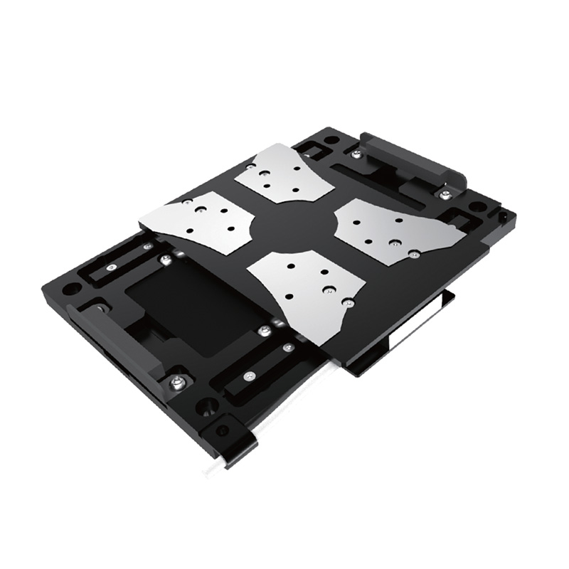
"This series comprises a range of modular, configurable precision motion stage solutions. We understand that different application scenarios have vastly different requirements for precision, speed, and environment. Therefore, we have designed four configuration levels, from Standard to Highly Customized, covering all scenario needs from rapid production line preliminary inspection to nanometer-scale defect inspection in high-vacuum environments.
Intelligent Selection Guide: Three Steps to Precise Positioning
1
Define Requirements
Minimum defect size?
Mask material specifications?
Inspection environment?
2
Match Bidirectional Repeatability
0.8μm → Standard Version
0.1μm → Advanced Version
0.05μm → High-End Version
3
Customize Adaptation
Advanced process / Phase shift mask
Special materials
Integration needs
Standard Version: Production Line Rapid Preliminary Inspection
- Suitable for: Production line rapid screening, customers with budget constraints
- Precision: ±0.8μm
- Motion Axes: X-axis scanning / XY plane positioning
- Core Advantages: Significant cost advantage, high delivery efficiency, flexible upgrade options
Advanced Version: Process Monitoring
- Suitable for: Mainstream production lines, process development and quality control
- Precision: ±0.1μm
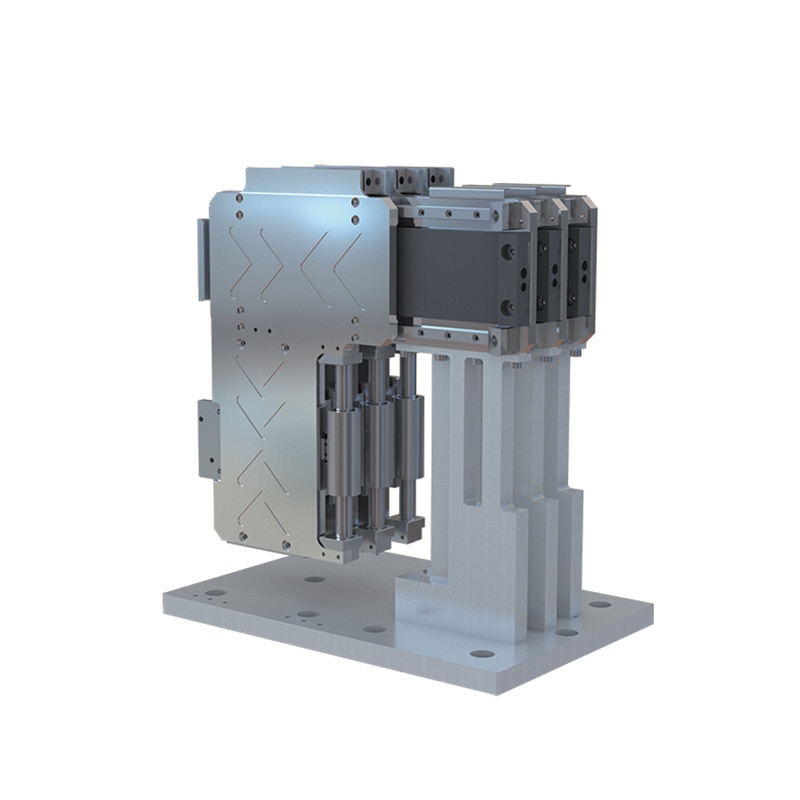
- Motion Axes: XYZT four-axis full inspection
- Core Advantages: Balanced precision, strong scalability, high repeatability
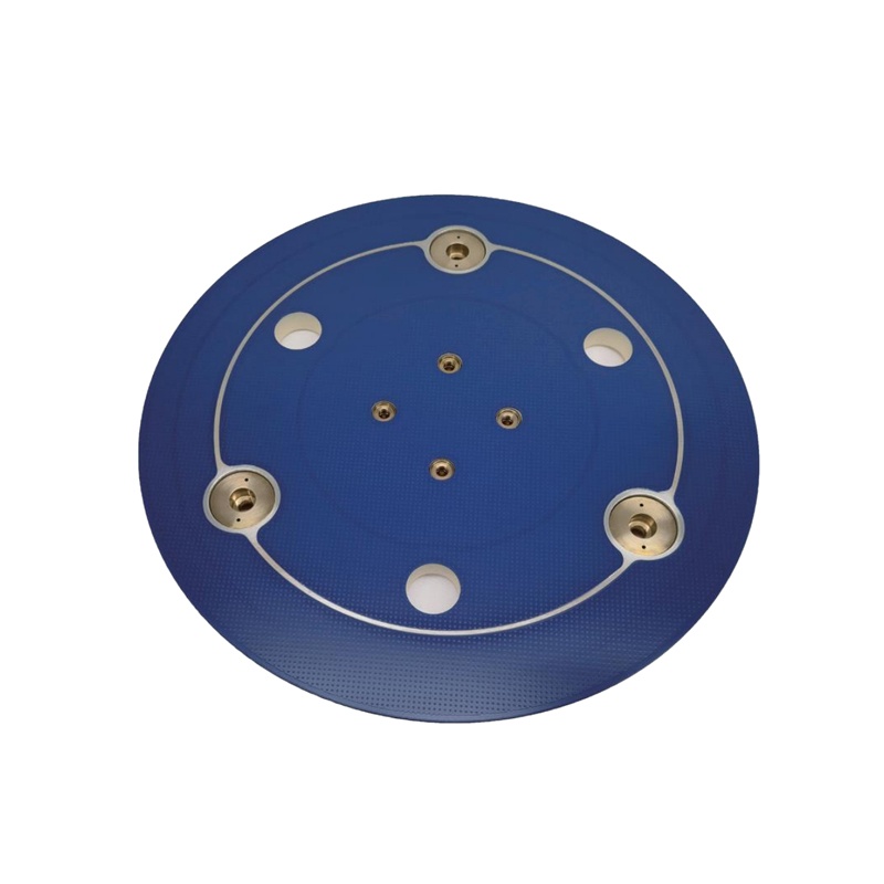
High-End Version: Nanometer-Scale Defect Inspection
- Suitable for: 7nm nodes / R&D centers, high-precision requirements
- Precision: ±0.05μm (Nanometer-level)
- Motion Axes: Six-axis linkage (XY + Z3T)
- Core Advantages: Nanometer-level resolution, multispectral imaging, high degree of automation
Highly Customized Version: Special Application Solutions
- Suitable for: Advanced masks, vacuum/cryogenic environments, national laboratories
- Features: Designed for extreme environments of advanced processes / phase shift masks
- Compatibility: Low thermal expansion materials, non-standard sizes
- Integration: Customer protocol interfacing, remote operation
- Core Advantages: Highly customized, solving the 5% of special requirements
Technology Upgrade Path: Scalable Growth
Start: Standard Version
Basic Architecture
→
Advance: Advanced Version
Higher Precision
Stronger Performance
→
Top-Tier: High-End Version
Nanometer-level Control
Excellent Performance
We understand that enterprise needs evolve. This series provides you with a clear product upgrade path. You can start with the Standard Version to meet basic needs. As process requirements advance, you can choose the Advanced Version to upgrade core inspection capabilities. For the most demanding nanometer-level requirements, the High-End Version is the ultimate choice. This "scalable growth" product philosophy aims to highly protect your investment plan.
From addressing the urgent need for rapid production line inspections to conquering the challenges of nanometer-scale detection, this series not only represents YiNGUAN Semiconductor's push towards the technological frontier but also underscores our commitment to the self-reliance of domestic semiconductor equipment.
We believe that through modular design and precise selection guides, we can help customers find the right "scalpel" to precisely position the future, between microns and nanometers.
1 Semiconductor Metrology & Inspection
Film Thickness / CD Metrology Overlay Metrology Mask Inspection Brightfield / Darkfield Defect Inspection Electron Beam Inspection
2 Semiconductor Wafer Manufacturing - High-End Equipment
Nanoimprint Lithography Laser Direct Writing
3 Semiconductor Advanced Packaging - Hybrid Bonding
Hybrid Bonding
4 Semiconductor Advanced Packaging - Other
TGV Thinning Machine Die Bonder Dicing Machine
Data Source Notes:
① Global Info Research:"Global and China Advanced Process Mask Industry Research and 14th Five-Year Plan Analysis Report": The advanced process mask market size is projected to reach $1.36 billion USD by 2031; The global advanced process mask market value was $591 million USD in 2024 and is projected to reach $1.36 billion USD by 2031, at a CAGR of 12.2% during the forecast period.